
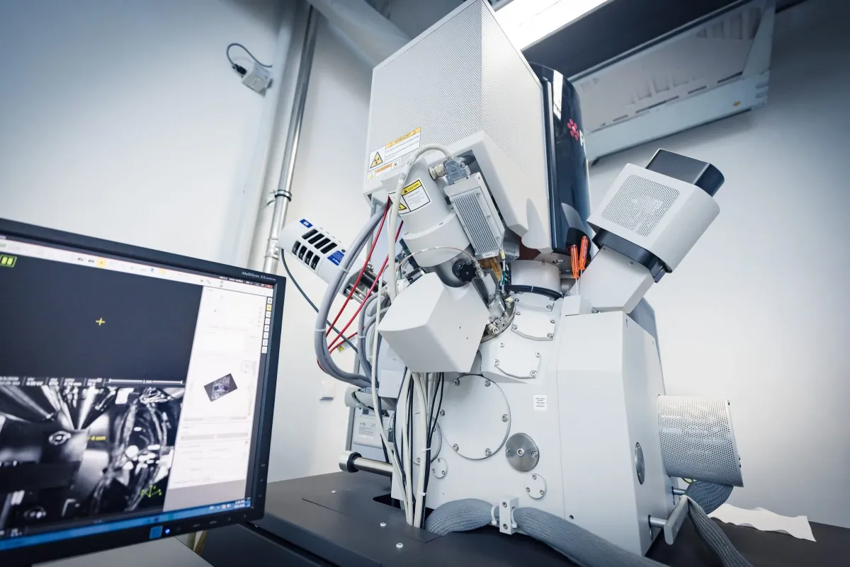
The electron microscopy lab at the Department of Chemistry is operated by the groups of Prof. Laquai and Prof. Müller-Caspary. It features high-resolution instruments for a great variety of applications in materials science. One key focus is the use and development of 4D STEM methods.
Titan Themis 60-300 (FEI)
Probe corrected, monochromated (scanning) transmission electron microscope
- Resolution around 100 pm in TEM and 80 pm in STEM mode
- Ultrafast electron detector for event based and time resolved (S)TEM, particularly suited for 4D STEM, Timepix T4 (Quantum Detectors)
- Energy dispersive X-ray (EDX) spectroscopy, Super-X detector
- Electron energy loss spectrometer: Gatan Enfinium ER /077
- Programmable phase plate with 48 pixels for electron beam shaping, AdaptEM WaveCrafter
- Various sample holders: tomography, heating, cooling and biasing, vacuum transfer and cryo transfer, among others
Helios G3 UC (FEI)
High resolution SEM with Ga ion column for focused ion beam sample manipulation.
- Landing energy range ~100 eV – 30 keV
- Resolution 0.6 nm (2 kV – 30 kV)
- Gas injection system for Pt deposition
- Oxford AZtec EDX detector
- Several detectors and imaging modes, sensitive for different sample aspects
- STEM possible (< 30 kV)
- Analysis of multilayer cross sections in-situ using Ga⁺ beam preparation
- Site-specific TEM lamella preparation
Tecnai G2 20 S-Twin (FEI)
Transmission electron microscopy with LaB6 emitter, operated at 200 kV.
- Tietz CMOS camera (2k)
- EDAX EDX detector
Further supportive instruments
- H₂/O₂ plasma cleaner, Gatan Solarus
- Ozone cleaner, ZoneTEM II Sunyu
- Instrumentation for mechanical sample preparation and for argon ion milling, Gatan PIPS
Key equipment
- Titan Themis 60-300 (FEI): resolution 100 pm in TEM and 80 pm in STEM mode; ultrafast electron detector for event based and time resolved (S)TEM, 4D STEM, Timepix T4 (Quantum Detectors); EDX; tomography, heating, cooling and biasing, vacuum and cryo transfer, and more
- Helios G3 UC (FEI): landing energy range ~100 eV – 30 keV; resolution 0.6 nm (2 kV – 30 kV); STEM possible (< 30 kV); in-situ Ga-beam preparation; site-specific TEM lamella preparation
- Tecnai G2 20 S-Twin (FEI): TEM with LaB6 emitter, operated at 200 kV; Tietz CMOS camera (2k); EDAX EDX detector